

Short answer: combine dissipation, charging and decay, and the dust problem becomes traceable
“The resistance result passes, so why does the part still attract dust?” It is one of the questions I hear most often in transparent antistatic projects. Usually the customer has not chosen the wrong material; the team has simply treated surface resistivity as the full answer. Resistivity is a still image. Film peel, robot pick-up, wiping and tray separation are the moving picture the part experiences every day.
A transparent plastic part exchanges charge when it contacts and separates from film, a cleanroom wipe, a rubber nozzle or another plastic part. The 10⁸–10¹⁰ Ω/□ surface resistivity of DGK-ABS KJD890TM establishes a dependable dissipation path. Once separation motion, grounding and local geometry are tuned around it, residual surface potential and dust attraction can be reduced together.
A mature validation report carries three lines of evidence that reinforce one another: peak potential under the intended motion, the way potential falls over time, and particle behavior under a common cleanliness and exposure condition. When all three point in the same direction, material selection, part optimization and production approval move much faster.
What surface resistivity, triboelectric voltage and charge decay each measure
| Metric | Question answered | Required records | Engineering value |
|---|---|---|---|
| Surface resistivity (Ω/□) | How readily charge can dissipate along the surface | Method, instrument, electrode, sample state, temperature, humidity, test voltage and read time | Establishes a stable material and batch baseline |
| Surface potential / voltage after rubbing (V) | How much potential is generated and retained after a defined interaction | Counter-material, contact load, cycles, speed, distance, polarity and peak | Finds the strongest charging action directly |
| Charge-decay time (s) | How long potential takes to fall from a defined start to a defined threshold | Start and end potentials, timing rule, grounding, humidity and repetitions | Shows how well material and grounding work together |
| Particle-attraction observation | Whether the real surface visibly attracts the target contamination | Particle type, size range, exposure, lighting, images and cleanliness baseline | Turns an electrical improvement into a visible result |
Normalize units before comparing results: surface resistance is normally reported in Ω, surface resistivity in Ω/□, volume resistivity in Ω·cm, voltage in V and decay time in s. Similar names do not indicate the same measured property.

Why parts within the same resistivity range can show different dust behavior
1. Counter-material and separation motion differ
Peeling film, lifting a vacuum nozzle, wiping and stacking parts create different contact areas, loads and separation speeds. Changing one variable can alter polarity and peak voltage, so the sample test should reproduce the real interaction.
2. Low humidity affects both charging and dissipation
Humidity changes surface moisture and available leakage paths. Condition samples at the customer's driest production condition, then repeat resistivity, voltage and decay with the same procedure. This locks in predictable dry-season performance early.
3. Part geometry and installation change the field
Thin edges, ribs, isolated regions, inserts and grounding-contact area can change local potential. Multi-location scanning on the real cover, tray or window often identifies the structural hot spot during the first trial.
4. Contamination, wiping and wear change the surface
Mold release, fingerprints, cleaner residue and repeated wiping affect resistance, charging and particle adhesion at the same time. Put before-and-after results on one trend sheet and surface stability becomes easy to see.
A four-layer validation path from material to real dust attraction
Our habit is to record the real work-cell motion before designing the test. A seemingly casual action—an operator peeling film quickly from the upper-right corner—can explain more than another round of plaque readings. The closer the procedure is to the work cell, the more effective the process adjustment becomes.
- Material: identify grade and batch, measure surface resistivity with full electrode and environmental records, and remove terminology or unit errors.
- Charging: use the real film, wipe, nozzle or mating part; fix load, cycles and separation speed; record polarity and peak surface voltage.
- Decay: under the same conditioning, record time from a defined starting potential to a defined threshold in free-standing, installed and intended-grounding states.
- Application: use a common cleanliness baseline, particles and exposure; image or count the result; relate dust behavior to the electrical measurements.
If the project also needs transmission, haze and wipe-durability testing, reuse the sample and report structure in the antistatic ABS resistance, transmission and durability guide, then add tribocharging and charge decay so electrical, optical and durability data form one complete evidence chain.
Why DGK-ABS KJD890TM is a strong starting point for clear, low-dust parts
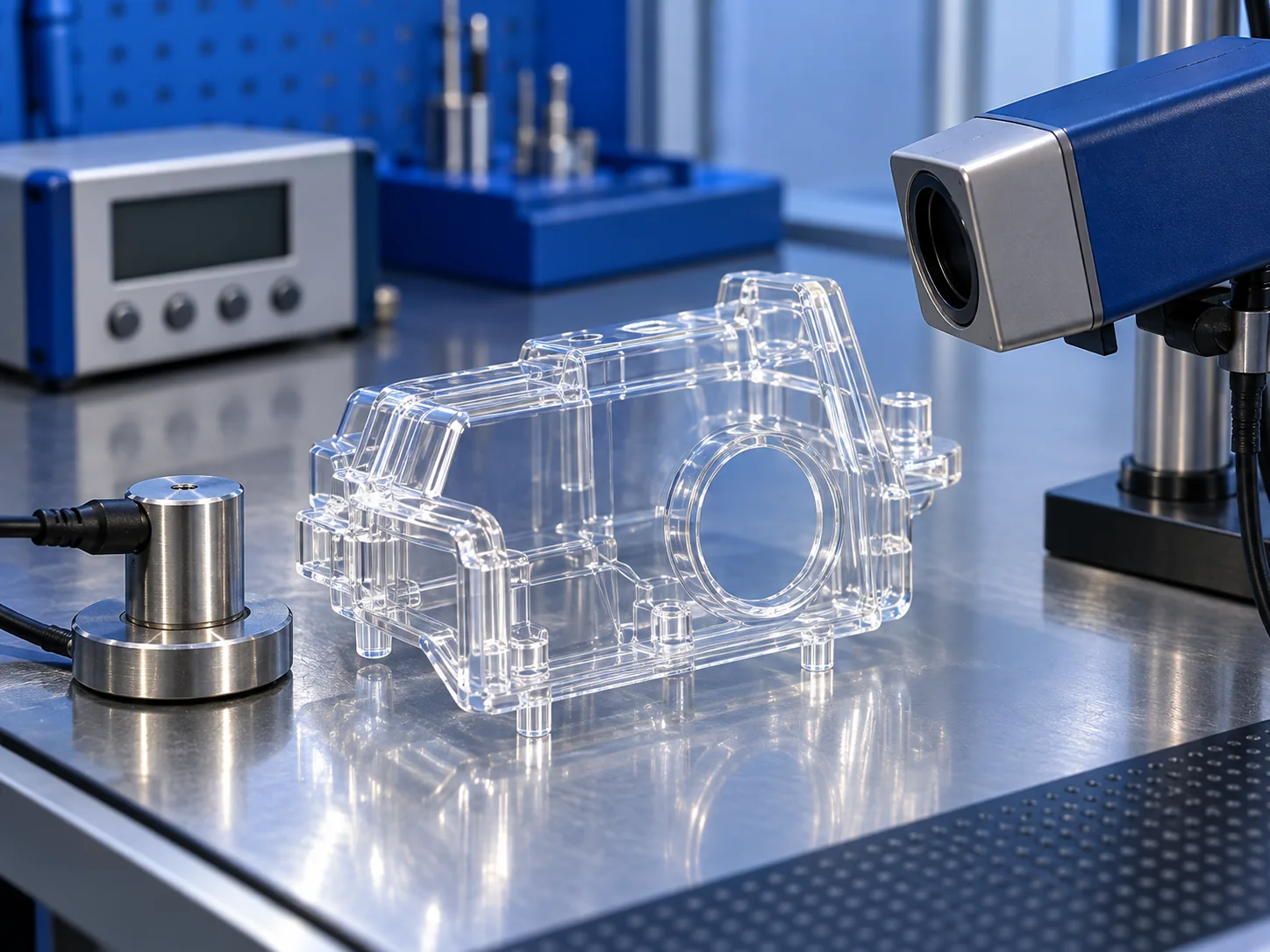
DGK-ABS KJD890TM combines high transparency, permanent antistatic performance and high-flow injection molding in one material system. Its 10⁸–10¹⁰ Ω/□ surface resistivity establishes the dissipation foundation, while a 48 g/10 min melt mass-flow rate supports complex clear geometries. Mechanical and thermal data let the team develop appearance, assembly and use-condition decisions in parallel.
| Data-sheet item | Reported value | Engineering use |
|---|---|---|
| Surface resistivity | 10⁸–10¹⁰ Ω/□, GB/T 1401-2002 | Builds a stable surface-charge dissipation foundation |
| Melt mass-flow rate | 48 g/10 min at 220°C/10 kg | Supports filling of thin walls, ribs and longer flow paths |
| Density | 1.118 g/cm³ | Part-mass and material-use estimates |
| Heat-deflection temperature | 85°C at 0.45 MPa | Guides the intended thermal use range |
| Flexural strength / modulus | 57 MPa / 1612 MPa | Supports stiffness assessment for housings, trays and panels |
| Tensile / yield strength | 39 MPa / 40.3 MPa | Supports snap-fit, frame and assembly design |
| Elongation at break | 35.8% | Material ductility reference |
| Notched impact strength | Charpy 10.5 kJ/m²; Izod 12.3 kJ/m² at 23°C | Supports handling, assembly and impact assessment |
| Molding starting points | Dry 85°C for 4–5 h; inject at 195–210°C; mold at 70°C | Trial start; machine, mold and part determine the final process |
Use these material values as the known base, then add part-specific transmission, haze, triboelectric voltage, charge decay and durability curves. This creates a direct path from material selection to a stable production window.
Three customer project reviews: from dust attraction to stable production
Case context: these anonymized composite cases combine experience from several projects. Customer identities and product details are removed while the engineering problem, decisions and outcome are retained.
Case 1: machine-vision cover—the material was sound; film peel and edge grounding were the real issue
Starting point. The customer molded a clear machine-vision cover so a camera could inspect an assembly inside. The first parts looked clean and surface resistivity was within the project range. Yet after half a shift, a fine ring of dust appeared in front of the lens. Operators wiped it more frequently, and the dust returned faster. The first reaction was to question the antistatic material and consider changing grades.
First investigation. When we received the cover and its production film, we reproduced the full unpacking sequence instead of starting with another plaque test: peel, pick up, wipe and install. The center of the cover dissipated consistently. The active area was the flange around the lens. Operators peeled quickly from one fixed corner, sweeping the separation front across that flange, while the flange sat electrically isolated from the main mounting point. A strong charging motion and a weaker local dissipation path were landing in the same place.
Engineering change. The team retained DGK-ABS KJD890TM, using its 10⁸–10¹⁰ Ω/□ surface resistivity as the electrical base and its 48 g/10 min flow to fill the thin flange. Molding began with 85°C drying for 4–5 h, 195–210°C injection and a 70°C mold. Packaging adjusted film-peel direction and speed, the part design created a more continuous path to the mounting ground, and cleaning standardized the wipe and one-way motion.
Outcome. On the second installation run, the concentrated dust ring was visibly reduced and dust returned more slowly after cleaning. The customer avoided an unnecessary material change and mold restart. The project closed with three practical production controls: a film-peel SOP, a four-point potential scan and an installation-ground check, then moved smoothly into pilot production.
Case 2: transparent chip tray—the center passed, but the stacking rim controlled the result
Starting point. The customer wanted a clear tray to improve chip identification and machine-vision inspection. Center readings stayed consistent, but after automated feeding, dust appeared along the rim and around a small number of pockets. Because the center still passed, production, quality and equipment teams looked in different directions—molding batch, ionization and cleanroom practice.
Testing the tray as a path. We stopped repeating the center measurement and placed points along both the resin flow path and equipment contact path: gate, mid-flow, flow end, chip pocket, stacking rim and robot pick zone. States expanded from one empty tray to empty, stacked separation, cover-film contact, robot pick and installed grounding. The pattern became clear: most of the tray dissipated consistently, while repeated separation at the stacking rim created the most variable charging event.
Two-sided adjustment. The material remained DGK-ABS KJD890TM, with the 85°C/4–5 h drying, 195–210°C injection and 70°C mold references anchoring a stable trial window. The molding team focused on the flow end and thin pockets. Automation adjusted lift timing, contact geometry and grounding. This combination was faster and more relevant than simply chasing a lower resistance number.
Outcome. Dust distribution became visibly more uniform during continuous feeding and the rim-localized issue came under control. Six critical locations became the incoming and batch-inspection standard, while “empty tray plus stacked separation” became the fixed test motion. Material, mold and automation teams were finally speaking from one data set, which accelerated production introduction. For the larger relationship among material, molding and CDM control, see the three transparent chip-tray failure modes.
Case 3: clear medical panel—turning “more wiping, more dust” into a manageable cleaning process
Starting point. This panel was cleaned every day, and the customer cared equally about visibility, low dust attraction and maintenance efficiency. During early use, shifts used different wipes, cleaner quantities and wiping directions. Some panels stayed clean; others collected fibers and fine dust soon after wiping. The material figures looked good, yet the floor result felt unpredictable.
Standardize motion before comparing material. The team fixed cleaner, wipe, load, cycle count and direction, then placed pre- and post-treatment resistivity, wipe-induced peak potential, decay trend and through-view appearance in one matrix. The 10⁸–10¹⁰ Ω/□ surface resistivity of DGK-ABS KJD890TM provided the stable electrical start. Its 39 MPa tensile strength, 40.3 MPa yield strength and 35.8% elongation also let the snap-fit and frame work continue in parallel.
From a material question to a process answer. Once the data was aligned, shift-to-shift variation stopped being mysterious. Fast back-and-forth wiping created a stronger short-term charging event, while cleaner residue changed the surface condition. The team moved to a one-way, controlled-load wipe with a short rest and appearance check. Production used the same method for inspection, and the customer used the same SOP in service.
Outcome. Dust return after cleaning improved visibly, the clear observation area stayed cleaner, and maintenance staff reduced repeated wiping. The customer gained more than a material grade: it gained a cleaning method that could be trained, sampled and traced. For medical devices, laboratory windows and frequently serviced clear covers, that repeatable method often creates more value than one isolated resistance figure.
Fast diagnostic matrix: start with the action that matches the symptom
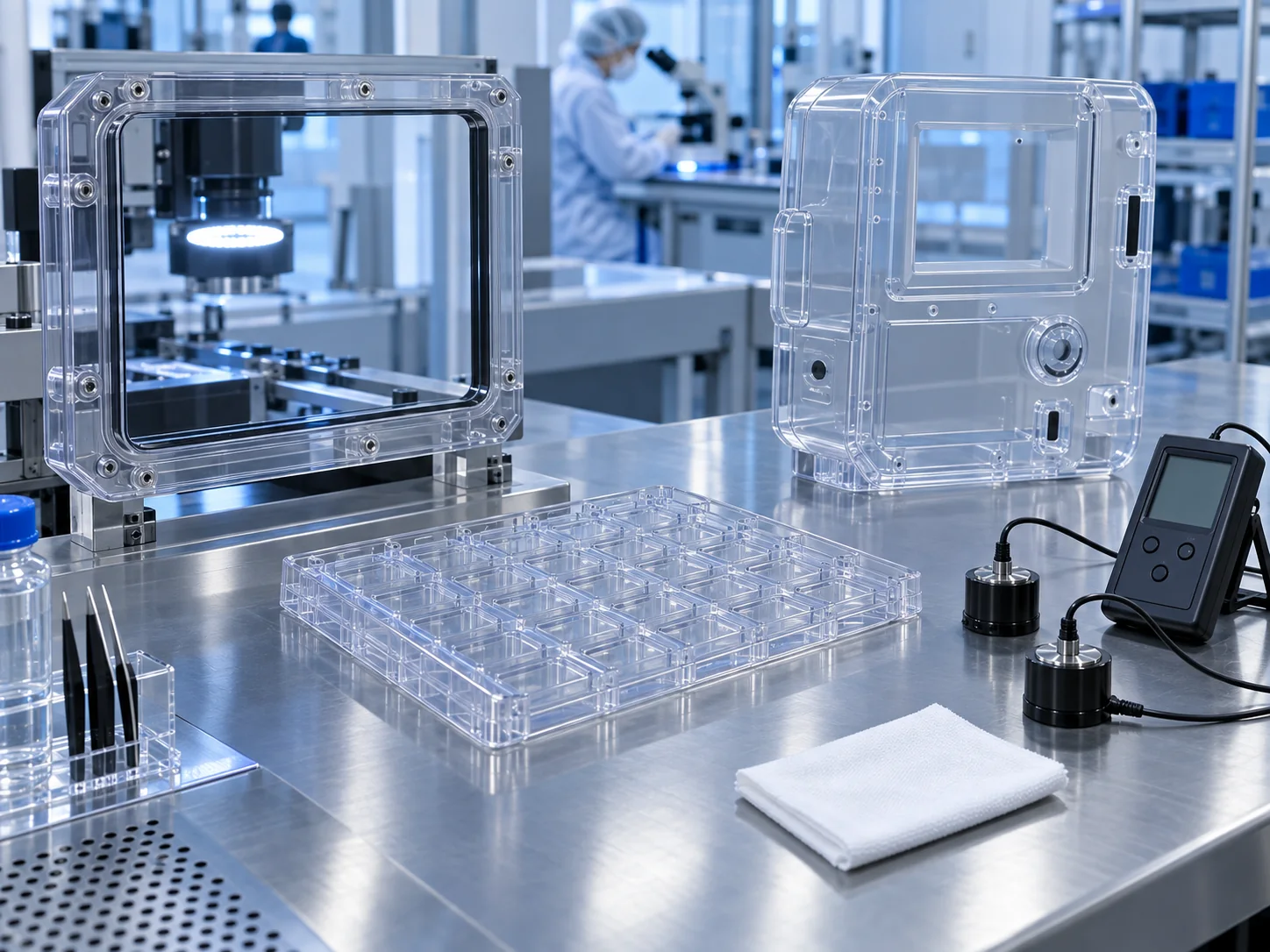
| Observed symptom | Check first | High-value action | Expected improvement |
|---|---|---|---|
| Dust appears immediately after film peel | Peel speed, angle and film | Fix the peel method and record peak potential | Find the strongest charging event and optimize packaging |
| Edges and ribs collect more dust than the center | Geometry, flow end and grounding continuity | Run a multi-point scan and adjust structure or ground contact | Reduce local high-potential areas |
| Winter variation is larger than summer | Minimum humidity and conditioning time | Build a dry-condition baseline and seasonal sampling plan | Keep year-round results predictable |
| Dust returns soon after wiping | Wipe, cleaner residue and motion | Standardize the cleaning SOP and compare before and after | Improve both cleaning efficiency and low charging |
| Plaques are stable but production parts vary | Drying, melt temperature, flow path and locations | Bind electrical results to each trial-molding revision | Create a repeatable molding window |
Acceptance checklist for reproducible, comparable and traceable data
| Validation item | Report record | Decision principle |
|---|---|---|
| Sample identity | Grade, batch, color, wall thickness, molding run and point ID | Keep material plaques and molded parts separate |
| Environment | Temperature, relative humidity, conditioning and cleanliness | Include the lowest relevant use humidity |
| Surface resistivity | Ω/□, method, instrument, electrode, test voltage and read time | Normalize the method before comparing location or batch |
| Tribocharging | Counter-material, load, cycles, speed, distance, peak and polarity | Reproduce the real contact-separation event |
| Charge decay | Starting potential, end threshold, timing and grounding state | Compare installed and uninstalled states, before and after exposure |
| Dust result | Particles, exposure, lighting, image or count method | Relate it directly to electrical data rather than one visual impression |
| Durability and production | Wiping, cleaning, wear, batch and process-change records | Recheck critical electrical and optical items after change |
Data and case notes
Material values come from the Clearastatic DGK-ABS KJD890TM data table reviewed on September 11, 2026. Units, test conditions and molding references follow the source table.
The three anonymized composite reviews organize the typical path from material screening and part testing to production optimization. A project report can use the matrices above to add its measured voltage, decay, optical and durability results.