

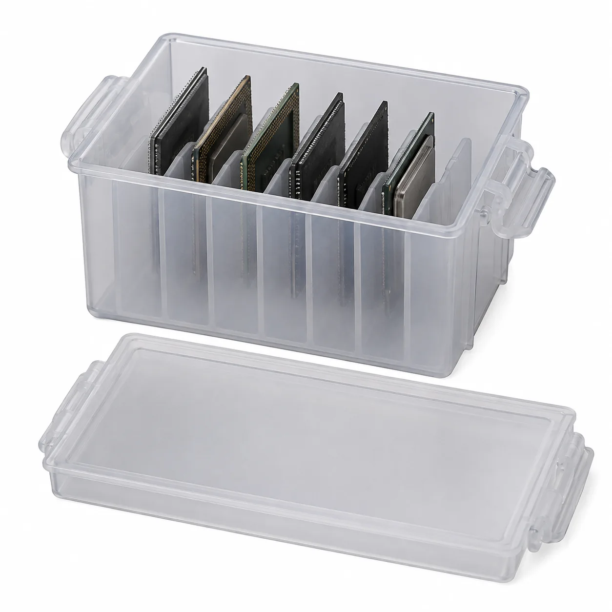
Typical Application Parts
Electronics and semiconductor customers are usually not buying a single antistatic material; they are solving static damage, particle contamination, slot identification and automated handling stability. Clearastatic starts with free samples to confirm surface resistance, clarity, haze and basic molding fit before moving into trial-batch material and mold trials.
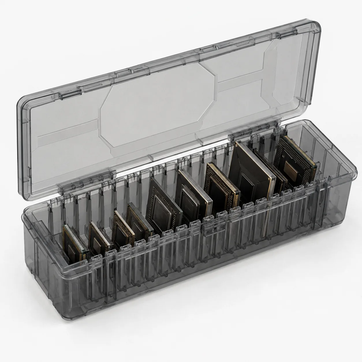
- IC trays, chip carriers and clear tray covers
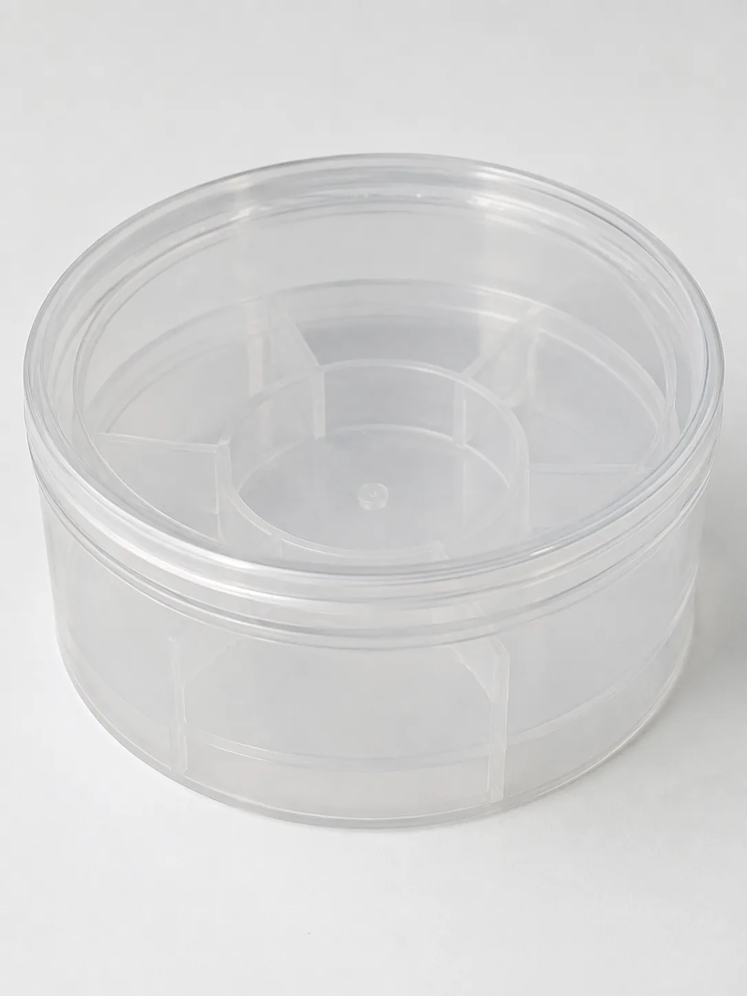
- Wafer-box windows, equipment panels and clear protective covers
- Cleanroom handling boxes, electronic component packaging and automated pick-and-place parts
Industry Requirements
Four risks to review first in electronics and semiconductor projects
Industry requirements, current pain points and corresponding solution routes are shown together so teams can quickly compare how transparent antistatic materials fit electronics and semiconductor applications.
| Industry Requirements | Current Pain Points | Clearastatic Matching Solution |
|---|---|---|
| ESD protection | Chip, component and carrier handling can create static adhesion, discharge and contamination risks. | Adjust the surface-resistance range to match trays, handling boxes, windows and protective covers. |
| Clean handling | Transparent parts can lose a clean appearance because of dust, oil stains or whitening after wiping. | Evaluate cleaning and appearance limits with transparent antistatic ABS, PMMA or other clear material routes. |
| Visual identification | Slot positions, labels, chip status and internal equipment status need direct visual confirmation. | Control clarity, haze and color so windows, clear covers and carriers remain easy to identify. |
| Automated pick-and-place | Tray warpage, dimensional variation and structural shrinkage can affect robotic pick-and-place and stacking. | Review material, tooling and injection-molding windows together to confirm wall thickness, locating boundaries and molding risks early. |
Performance Metrics
Performance Advantages
The five data points most often needed early in transparent antistatic projects are shown together so purchasing, R&D and tooling teams can align quickly.

85%
Clarity
Suitable for windows, clear covers, label identification and visual confirmation of internal status.

108
Antistatic Level
Confirm the antistatic range by surface-resistance target to reduce static adhesion and ESD risk.

12.3KJ/㎡
Impact Strength
Used to evaluate impact resistance during handling, pick-and-place, assembly and equipment protection.

39MPa
Tensile Strength
Tensile method: 50 mm/min, GB/T1040-2006.
48g/10min
Melt Index
Used to judge processing windows for injection molding, extrusion, thermoforming and mold trial stages.
Customization is available for ESD targets, clarity, clean appearance, tray structure and molding process.
ESD and cleanliness metrics
- Surface Resistance
- Dust Adhesion
- Clarity / haze
- Wiped appearance
Carrier validation path
- Sample testing
- 5 kg pilot trial
- Mold trial pick-and-place
- Stacking retest
Engineering Deliverables
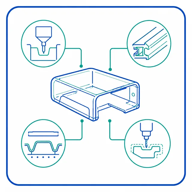
- Material Route
- ESD target
- DFM Points
- Molding Window
Production introduction coordination
- Materials Engineer
- Tooling Engineer
- Injection Molding Engineer
- Quality Inspection
Quotation Plan
Transparent Antistatic Material Quotation Plan
For custom transparent antistatic electronics and semiconductor products, Clearastatic separates quotation into free samples, pilot trial, final trial and tooling cost so customers can control validation cost and gradually lock the production route.
Free Samples
Used to test conductivity, clarity, haze and basic appearance during early transparent antistatic material selection.
Samples are freeTrial-batch Material
Trial-batch transparent antistatic material is CNY 45/kg. A 5 kg pack is available for mold trials, trial production and small-batch retesting.
CNY 45/kg, from 5 kgFinal Trial Formula
The final trial locks the exclusive formulation and confirms the production window by color, clarity, antistatic level, base resin and process.
about 45-CNY 48/kgTooling Cost Consultation
Tooling cost is evaluated separately by part size, structure, cavities, polishing grade, trial requirements and delivery schedule.
Quoted by productFAQ
FAQ
These questions cover material selection, sample testing, trial-batch validation, quotation and tooling review so the next step can be confirmed early in the project.
Why do chip trays and IC handling boxes need transparent ESD materials?
During handling, inspection and storage, chips, ICs and precision electronic components need static control, internal material visibility and surface cleanliness at the same time.
Ordinary transparent plastics can accumulate static electricity and attract dust, while traditional conductive materials are often not very clear. Transparent antistatic materials are better suited for chip trays, IC handling boxes, ESD-safe transparent covers, inspection fixtures and equipment observation windows where visibility and ESD control are both required.
What antistatic level should be selected for a chip tray?
The resistance range cannot be decided only from the product name “chip tray”.
Selection should consider the ESD sensitivity of the device, contact method, handling environment and the customer’s internal ESD standard.
For trays and carriers that require faster charge dissipation, a lower surface-resistance range may be considered. For transparent parts that place more emphasis on visibility and static-buildup control, the antistatic level and transparency need to be balanced.
The final recommendation should be confirmed through testing on actual molded parts.
Will transparency become worse as the antistatic level becomes stronger?
There is usually a balance between antistatic performance and transparency.
The material system, additive ratio, part thickness and base resin all affect the final surface resistance, light transmission and haze.
Transparent antistatic material development should therefore not define only one resistance value. It should confirm the target surface resistance, light transmission, haze, product thickness and appearance requirements together before matching the formulation to the actual product.
Will transparent antistatic materials bloom, shed powder or contaminate electronic components?
For chip, IC and precision electronic component carriers, material selection must consider not only antistatic performance but also blooming, migration, surface cleanliness and particles generated by friction.
For applications with higher cleanliness requirements, additional validation is recommended based on the actual use environment, such as surface cleanliness, wiping, volatile substances or particle-related testing.
Whether a material is suitable for semiconductor use cannot be judged by surface resistance alone.
Why can the resistance of an injection-molded tray change even when the material test passes?
The final antistatic performance of a molded part is not determined by the raw material alone.
During injection molding, molding temperature, shear, flow distance, wall thickness, gate location, material dispersion and mold structure can all affect the performance at different positions of the final part.
For chip trays, clear handling boxes and complex electronic components, actual injection-molded part testing is recommended instead of relying only on test data from raw material pellets.
What should be tested during semiconductor and electronics sampling?
Testing should focus on the actual use scenario of the product:
- Surface resistance: confirm whether the target ESD level is reached.
- Light transmission and haze: determine whether internal device identification meets requirements.
- Humidity stability: observe changes in antistatic performance under different environments.
- Wiping stability: verify performance retention after alcohol or cleaning.
- Injection appearance and flowability: check flow marks, silver streaks, short shots and clear appearance.
- Actual molded-part performance: confirm resistance, dimensions and appearance after injection molding.
For formal projects, the validation result of the actual molded part should be used as the final basis for material selection.